
High-Frequency Characterization and Modeling of GaN Transistors
Principal Investigator: Professor Fay
AWaRE REU Researcher: Lauren Stark, University of Notre Dame
Other Contributor: Nivedhita Venkatesan
Project Summary:
GaN-based transistors are increasingly attractive for applications across the microwave and millimeter-wave frequency range, including power amplifiers, low-noise amplifiers, switches for reconfigurable RF systems, and more. This project includes measuring the performance of several GaN transistor designs (including DC measurement, low-frequency AC, and high-frequency on-wafer characterization) and developing models suitable for computer-aided circuit design of these transistors from the measured characteristics. Comparisons of different models (e.g. ASM-HEMT, Angelov, etc.) and their respective abilities to capture key device performance features are included to evaluate the suitability of the models for different circuit applications.
Finding:
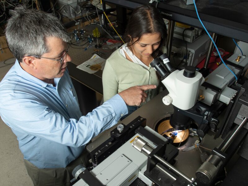
Transistors are the workhorse device that underpins all modern electronics. While silicon-based transistors have come to dominate in digital applications due to their scalability and high degree of integration, for wireless communications and RF applications, silicon devices have limitations in terms of their output power, frequency range, and noise performance. One attractive solution to this problem that is being explored is the use of Gallium Nitride (GaN) based transistors. Because of the material properties of GaN (larger band gap, higher electron mobility) GaN transistors have the ability to function at a higher power levels, higher frequencies, and at higher temperatures than silicon. However, an open question is what are the ultimate limits of GaN transistors, and how can they best be used in circuits? To address this question, a nonlinear model (suitable for circuit design) is being extracted based on measured electrical characteristics of devices. Example research-grade GaN transistors, with gate lengths of approximately 50 nm and gate periphery of 37.5 microns, were placed under a microscope on a probe station. Two microwave-style probes were used (one on each side) that allowed different voltages to be applied to the device, and the resulting currents to be measured. The outcome of this test created multiple data sets that quantify the device’s response to these applied measurements.